| 产品特性:TFT彩屏 | 加工定制:是 | 品牌:鑫洪泰 HOT DISPLAY HOTLCD |
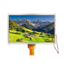
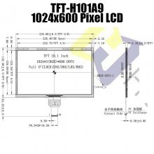
| 型号:TFT-H101A9 | 种类:TFT型液晶屏(模块) | 屏幕尺寸:10.1英寸 |
| 色彩:全彩 | 亮度:1000cd/m2 | 分辨率:1024*600 |
| 可视角度:IPS全视角° | 接口:LVDS |

10.1寸TFT彩屏LVDS/RGB接口LCD显示屏工业电脑面板液晶屏
General Feature
| Item | Standard Value | Unit |
| Display Size | 10.1 | Inch |
| Number of Pixels | 1024(H)*3(RGB)* 600(V) | dots |
| Active Area | 222.72(H)* 125.28(V) | mm |
| Outline Dimension | 235.00(H) * 143.00(V) * 5.30(D) | mm |
| Viewing Direction | FULL O'clock | - |
| TFT Interface | LVDS/RGB | - |
| TFT Driver IC | EK79001+EK73215 | - |
TFT Driver Condition | VCI=3.3V(Typ) | V |
| Backlight | White LED/42 PCS/6 LEDs serial 7 ways parallel | - |
| Touch Panel | Without TP | - |
| CTP Driver IC | - | |
| CTP Driver Condition | VDD=3.3V(Typ) | V |
| Operation Temperature | -30 ~ 80 |
|
| Storage Temperature | -35 ~ 85 |
|
TFT Pin Description
| Pin NO. | Symbol | Description |
| 1 | VCOM | TFT Common Electrode Voltage |
| 2~3 | VCI | Digital Power |
| 4 | NC | No Connect |
5 | RESX | Global reset pin. Active low to enter reset state. Usually pulled high. For stability, an RC delay circuit needs to be connected externally. (RESX delay VCI greater than 1ms) |
|
STBYB | Standby mode, normally pull high. STBYB = "VCI", normal operation STBYB = “GND”, Standby mode |
| 7 | GND | Ground |
| 8 | D0N | LVDS negative differential data |
| 9 | D0P | LVDS positive differential data |
| 10 | GND | Ground |
| 11 | D1N | LVDS negative differential data |
| 12 | D1P | LVDS positive differential data |
| 13 | GND | Ground |
| 14 | D2N | LVDS negative differential data |
| 15 | D2P | LVDS positive differential data |
| 16 | GND | Ground |
| 17 | DCKN | LVDS negative differential clock |
| 18 | DCKP | LVDS positive differential clock |
| 19 | GND | Ground |
| 20 | D3N | LVDS negative differential data |
| 21 | D3P | LVDS positive differential data |
| 22 | GND | Ground |
| 23~24 | NC | No Connect |
| 25 | GND | Ground |
| 26~27 | NC | No Connect |
28 | HSD | Data channel selection STBYB = "VCI", 6 bit STBYB = “GND”, 8 bit |
| 29 | AVDD | Analog Power |
| 30 | GND | Ground |
| 31~32 | LEDK | LED Cathode,Not connected here |
33 |
L/R | Horizontal scan direction control pin L/R= "VCI", From left to right(Default) L/R= “GND”, From right to left |
34 |
U/D | Vertical scan direction control pin U/D= "VCI", From down to up. U/D= “GND”, From up to down.(Default) |
| 35 | VGL | TFT Gate OFF Voltage |
| 36~37 | NC | No Connect |
| 38 | VGH | TFT Gate ON Voltage |
| 39~40 | LEDA | LED Anode,Not connected here |